As semiconductor technologies evolve, substrates and wafers are becoming increasingly thinner, pushing the limits of conventional handling systems. At the same time, customer expectations and process requirements are growing rapidly, demanding higher precision, flexibility and reliability across all production stages.
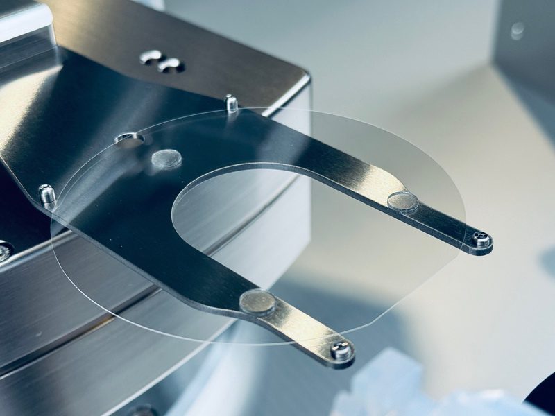
Adenso addresses these challenges with its latest innovation: UltraThin.Handling (UTH) solutions, engineered for substrates down to 30 microns thickness in formats such as 125 x 125 mm – ideal for applications including Quantum Chips, Photonic Integrated Circuits (PIC), and advanced packaging.
Meeting the challenge of ultra-thin materials
Handling ultra-thin substrates introduces a new level of complexity:
- Increased fragility and deformation risk
- Strict alignment and positioning tolerances
- Sensitivity to thermal and mechanical stress
- Integration into increasingly complex process flows
Standard automation solutions are often not designed to meet these demands. This is where Adenso’s expertise and VAC.ROBOTICS platform make a decisive difference.
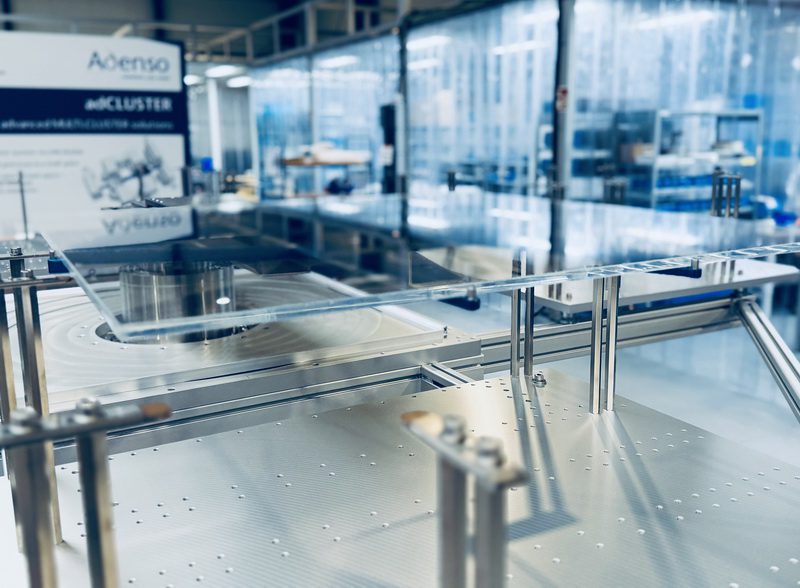
Built on the proven VAC.ROBOTICS platform
Adenso’s UltraThin.Handling solutions are based on the powerful and versatile VAC.ROBOTICS platform, allowing users to seamlessly integrate ultra-thin substrate handling into established environments: both atmospheric (ATM) and vacuum (VAC) conditions.
This means you benefit from a familiar, modular system while extending its capabilities to the most delicate materials.
Full Process Capability, even for the Thinnest Substrates
With Adenso UTH.solutions, you can perform a wide range of critical processes without compromising substrate integrity:
- Align: High-precision positioning for ultra-thin wafers
- Flip: Safe and controlled inversion of fragile substrates
- Bond: Reliable integration into packaging workflows
- Heat: Controlled thermal processing with minimal stress
- Test: Integration into inspection and testing sequences
… and more
All steps are optimized to ensure maximum process stability and yield, even at extreme thicknesses.
Designed for future technologies
Ultra-thin wafer handling is becoming essential in cutting-edge applications such as:
- Quantum Computing: Handling delicate Quantum Chips with extreme care
- Photonics (PIC): Enabling precise processing of photonic substrates
- Advanced Packaging: Supporting next-generation integration concepts (e.g. chiplets, heterogeneous integration)
Adenso’s UTH.solutions are designed to meet not only today’s requirements, but also the needs of tomorrow’s breakthrough technologies.
Be Prepared for What’s Next
As the industry continues to evolve, the ability to handle ultra-thin substrates efficiently and safely will become a key competitive advantage.
Be prepared with Adenso’s UltraThin.Handling solutions.
Learn more: www.ultrathin.solutions
What ultra-thin handling challenges are you currently facing?
Let’s solve them together.